An electronic lock or digital lock is a device which has an electronic control assembly attached to it. They are provided with an access control system. This system allows the user to unlock the device with a password. The password is entered by making use of a keypad. The user can also set his password to ensure better protection. The major components include a keypad, LCD and the controller AT89C51 which belongs to the 8051 series of microcontrollers. This article describes the making of an electronic code lock using the 8051 microcontroller.
DESCRIPTION :
A 4x3 matrix keypad and a 16x2 LCD have been used here. Keypad and LCD are very commonly used input & output devices, respectively. A four digit predefined password needs to be specified the user. This password is stored in the system.
While unlocking, if the entered password from keypad matches with the stored password, then the lock opens and a message is displayed on LCD. Also an output pin is made high to be used for further purpose.
The connections in the circuit are as following: port P2 of microcontroller AT89C51 is used as data input port which is connected to data pins (7-14) of LCD. P1^0, P1^1 and P1^2 pins of microcontroller are connected to control pins RS, RW and EN of LCD. Port P0 is used to take input from keypad. P0^7 has been used as lock output pin of controller.
As the program starts, string ‘Enter Password’ is displayed on LCD. The keypad is scanned for pressed digits one by one. Every time, row and column of the key pressed is detected and a ‘*’ is displayed on LCD corresponding to the entered number. After the four digits are entered, the user is prompted to ‘Confirm Password’ and again the input is taken through LCD. If the passwords do not match, a message is displayed to indicate ‘Wrong Password’; otherwise the user is prompted to unlock the device.
To unlock, user needs to ‘Enter Password’ through keypad. Again the keypad is scanned for pressed keys and corresponding digits are identified. The passkey is displayed as ‘****’ on the LCD screen. After the four digits are entered, they are compared with the pre-set password. If all the four digits match with set password, LCD displays ‘Lock Open’ and the lock output pin goes high. If the security code is wrong, ‘Wrong Password’ is sent to be displayed on LCD. The system gets locked if more than three attempts are made with wrong password to open the electronic lock. The system needs to be reset in such a case.
CIRCUIT DIAGRAM :
CIRCUIT DIAGRAM :

VIDEOS :
COMPONENTS :
preset :
A preset is a three legged electronic component which can be made to offer varying resistance in a circuit. The resistance is varied by adjusting the rotary control over it. The adjustment can be done by using a small screw driver or a similar tool. The resistance does not vary linearly but rather varies in exponential or logarithmic manner. Such variable resistors are commonly used for adjusting sensitivity along with a sensor.
The variable resistance is obtained across the single terminal at front and one of the two other terminals. The two legs at back offer fixed resistance which is divided by the front leg. So whenever only the back terminals are used, a preset acts as a fixed resistor. Presets are specified by their fixed value resistance.
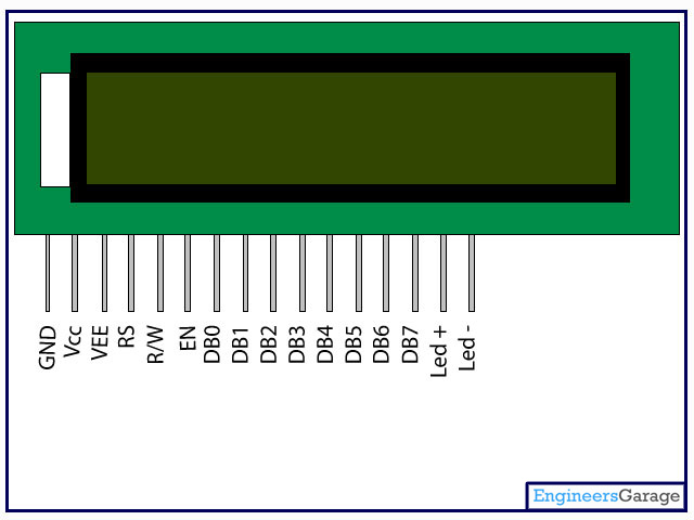
Pin Diagram:

LCD
LCD (Liquid Crystal Display) screen is an electronic display module and find a wide range of applications. A 16x2 LCD display is very basic module and is very commonly used in various devices and circuits. These modules are preferred over seven segments and other multi segment LEDs. The reasons being: LCDs are economical; easily programmable; have no limitation of displaying special & even custom characters (unlike in seven segments), animations and so on.
A 16x2 LCD means it can display 16 characters per line and there are 2 such lines. In this LCD each character is displayed in 5x7 pixel matrix. This LCD has two registers, namely, Command and Data.
The command register stores the command instructions given to the LCD. A command is an instruction given to LCD to do a predefined task like initializing it, clearing its screen, setting the cursor position, controlling display etc. The data register stores the data to be displayed on the LCD. The data is the ASCII value of the character to be displayed on the LCD. Click to learn more about internal structure of a LCD.
Pin Diagram:

Pin Description:
Pin No
|
Function
|
Name
|
1
|
Ground (0V)
|
Ground
|
2
|
Supply voltage; 5V (4.7V – 5.3V)
|
Vcc
|
3
|
Contrast adjustment; through a variable resistor
|
VEE
|
4
|
Selects command register when low; and data register when high
|
Register Select
|
5
|
Low to write to the register; High to read from the register
|
Read/write
|
6
|
Sends data to data pins when a high to low pulse is given
|
Enable
|
7
|
8-bit data pins
|
DB0
|
8
|
DB1
| |
9
|
DB2
| |
10
|
DB3
| |
11
|
DB4
| |
12
|
DB5
| |
13
|
DB6
| |
14
|
DB7
| |
15
|
Backlight VCC (5V)
|
Led+
|
16
|
Backlight Ground (0V)
|
Led-
|
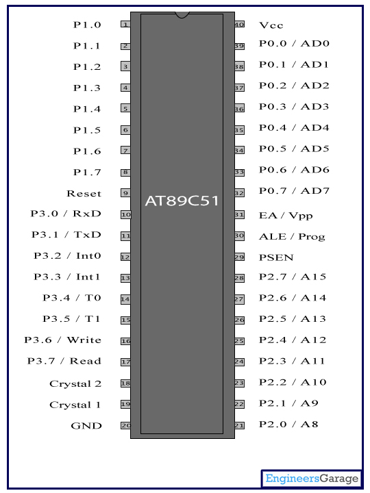
AT89C51 Microcontroller

AT89C51 is an 8-bit microcontroller and belongs to Atmel's 8051 family. ATMEL 89C51 has 4KB of Flash programmable and erasable read only memory (PEROM) and 128 bytes of RAM. It can be erased and program to a maximum of 1000 times.
In 40 pin AT89C51, there are four ports designated as P1, P2, P3 and P0. All these ports are 8-bit bi-directional ports, i.e., they can be used as both input and output ports. Except P0 which needs external pull-ups, rest of the ports have internal pull-ups. When 1s are written to these port pins, they are pulled high by the internal pull-ups and can be used as inputs. These ports are also bit addressable and so their bits can also be accessed individually.
Port P0 and P2 are also used to provide low byte and high byte addresses, respectively, when connected to an external memory. Port 3 has multiplexed pins for special functions like serial communication, hardware interrupts, timer inputs and read/write operation from external memory. AT89C51 has an inbuilt UART for serial communication. It can be programmed to operate at different baud rates. Including two timers & hardware interrupts, it has a total of six interrupts.
Pin Diagram:

Pin Description:
Pin No
|
Function
|
Name
| ||
1
|
8 bit input/output port (P1) pins
|
P1.0
| ||
2
|
P1.1
| |||
3
|
P1.2
| |||
4
|
P1.3
| |||
5
|
P1.4
| |||
6
|
P1.5
| |||
7
|
P1.6
| |||
8
|
P1.7
| |||
9
|
Reset pin; Active high
|
Reset
| ||
10
|
Input (receiver) for serial communication
|
RxD
|
8 bit input/output port (P3) pins
|
P3.0
|
11
|
Output (transmitter) for serial communication
|
TxD
|
P3.1
| |
12
|
External interrupt 1
|
Int0
|
P3.2
| |
13
|
External interrupt 2
|
Int1
|
P3.3
| |
14
|
Timer1 external input
|
T0
|
P3.4
| |
15
|
Timer2 external input
|
T1
|
P3.5
| |
16
|
Write to external data memory
|
Write
|
P3.6
| |
17
|
Read from external data memory
|
Read
|
P3.7
| |
18
|
Quartz crystal oscillator (up to 24 MHz)
|
Crystal 2
| ||
19
|
Crystal 1
| |||
20
|
Ground (0V)
|
Ground
| ||
21
|
8 bit input/output port (P2) pins
/
High-order address bits when interfacing with external memory
|
P2.0/ A8
| ||
22
|
P2.1/ A9
| |||
23
|
P2.2/ A10
| |||
24
|
P2.3/ A11
| |||
25
|
P2.4/ A12
| |||
26
|
P2.5/ A13
| |||
27
|
P2.6/ A14
| |||
28
|
P2.7/ A15
| |||
29
|
Program store enable; Read from external program memory
|
PSEN
| ||
30
|
Address Latch Enable
|
ALE
| ||
Program pulse input during Flash programming
|
Prog
| |||
31
|
External Access Enable; Vcc for internal program executions
|
EA
| ||
Programming enable voltage; 12V (during Flash programming)
|
Vpp
| |||
32
|
8 bit input/output port (P0) pins
Low-order address bits when interfacing with external memory
|
P0.7/ AD7
| ||
33
|
P0.6/ AD6
| |||
34
|
P0.5/ AD5
| |||
35
|
P0.4/ AD4
| |||
36
|
P0.3/ AD3
| |||
37
|
P0.2/ AD2
| |||
38
|
P0.1/ AD1
| |||
39
|
P0.0/ AD0
| |||
40
|
Supply voltage; 5V (up to 6.6V)
|
Vcc
| ||


3 comments:
Nice your blog.........
Smart samsung door lock singapore mechanism accommodates each person’s person lifestyle with all the different access methods.
please send me the code on my mail
ijazwazir94@gmail.com
Thanks
Ooooh we love your blog! Very well written
Post a Comment